Our Products
We offer a complete product range of PCB Double Side Board, Multilayer PCB Board and PCB Single Side Boards

Double-sided printed circuit boards have wiring patterns on both sides of the insulating material, i.e. the circuit pattern is available both on the components side and the solder side. Obviously, the component density and the conductor lines are higher than the single-sided boards.
Double-sided PTH board has circuitry on both sides of an insulating substrate, which is connected by metallizing the wall of a hole in the substrate that intersects the circuitry on both sides. This technology, which is the basis for most printed circuits produced, is becoming popular in cases where the circuit complexity and density is high.
Double-sided non-PTH board is only an extension of a single-sided board. Its cost is considerably lower because plating can be avoided. In this case, through contacts are made by soldering the component leads on both sides of the board, wherever required. In the layout design of such boards, the number of solder joints on the component side should be kept to a minimum to facilitate component removal, if required. It is generally recommended that conductors should be realized as much as possible on the non-component side and only the remaining should be placed on the component side.

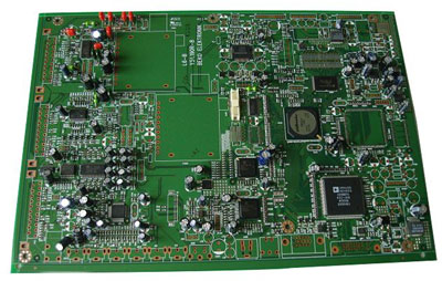
A multilayerPCBboard is used in situations where the density of connections needed is too high to be handled by two layers or where there are other reasons such as accurate control of line impedances or for earth screening.
A multilayerPCBcontains two reference planes and a signal via. The signal via allows a signal to flow through all the planes. A stitching via is connected to one of the planes next to the signal via and serves to reduce the area through which the signal passes through. This is very important as it may assist in reducing noise and cross talk.
The electrical circuit is completed by interconnecting the different layers with plated through-holes, placed transverse to the board at appropriate places. Multi-layer boards have three or more circuit layers, while some boards have even as many as 50 layers.
Advantages of multilayer PCBs include high reliability and uniform wiring. However, the initial costs are higher than that of one-layered PCBs. Also, repairing a multilayerPCBis quite difficult.