Explore Our Products
We are happy to fulfill your requirements.
Please let us know your sourcing needs.
Please let us know your sourcing needs.


Welcome to SKTECH ENTERPRISE LIMITED
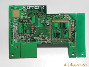
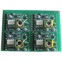
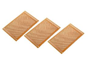
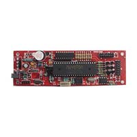
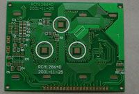
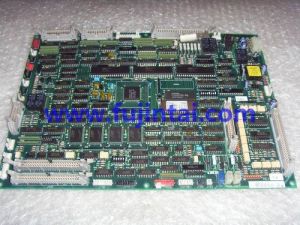
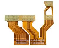
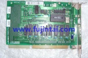
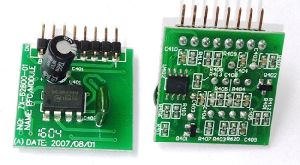
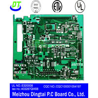
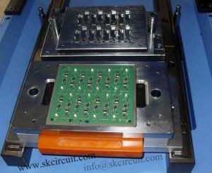
Welcome to SKTECH , an established supplier of printed circuit boards(PCBs) and punching tool in Shenzhen, China. With years of development, SkTech has been a expert in pcb and punching tool with better solutions and one-stop services. Our strong focus on customer service and technical leadership, as well as the quality and on-time delivery of our high technology PCBs and PUNCHING TOOLs has allowed SKTECH to build and maintain our reputation in whole world.
-

Sales manager
Ramona chan
-

Year of Establishment
2010
-

Primary Business
Supplier
-

Number of Employees
101 - 250
-

Annual Turnover
USD 5 to 10 Million Approx.