Our Products
Our offered Product range includes Op-Amp IC 741 Application and Characteristics (Parameter) Trainer SB-913, P,PI,PID Control System- Temperature Control SE-1027, 4:1 Multiplexer & 1:4 Demultiplexer SD-311, Signal Generator Demonstrator SE-806 and QAM Modulation & Demodulation SB-224.

The Trainer has DC 0-12V/500mA (1 No.) Variable Power supply, Solar Cell of @ 6V mounted on the Panel , Variable light intensity applied to the sell to study its V-I characteristics and Test Points for connecting the meters in circuit.
Objectives :
Accessories Included :
 Modulation and Demodulation Using PLL IC 565 SA-216")
FM Modulation - The monolithic function generator IC and Op-Amp IC 741 as non-inverting amplifier wired with Resistors & Capacitors to generate carrier internally and to provide Frequency modulated (FM) output for applied modulating input. facility to adjust the modulation index. fixed Carrier frequency about 1 MHz generated internally. FM Demodulation: The PLL IC 565 wired with RC network and higher order filter to form a FM demodulation circuit using PLL IC to provide demodulated output for applied FM input. FM detector bandwidth upto 3KHz, facility to change the VCO free running and locking frequency. Built-in fixed DC ±12V/500mA Power supply and maximum test points for studying the experiments.
Objectives :
Accessories Included :

SSB-SC Modulation - The circuit has two Balance modulators wired using IC 1496, two 900 RC Phase shift networks and OP-AMP IC 741 as summing amplifier. The external modulating signal and carrier signal are applied as an inputs directly to one Balance modulator and through 900 RC phase shifter to another Balance modulator to provide Balance modulator output which after summing network provides SSB-SC AM Balance modulator output. Maximum modulating frequency 10KHz, Maximum carrier frequency 100KHz, Built-in fixed DC ±12V/500mA Power supply and maximum test points.
SSB-SC Demodulation - The circuit uses IC 1496 wired with RC components and filter network as a SSB-SC Balance Demodulator to provide the demodulated AF output for the applied SSB-SC input. Maximum modulating frequency 10KHz, Maximum carrier frequency 100KHz, Bandwidth 3KHz, Built-in fixed DC +12V/500mA Power supply and maximum test points. Sine wave signal generators (2Nos) variable upto 100KHz frequency and 10Vpp amplitude.
Objectives :
Accessories Included : Set of Patch Cords, Operating Manual.
 Modulation and Demodulation SA-247")
TDM-PAM Modulation - This has two PAM modulators and two channel analog TDM Modulator wired as TDM PAM modulator. Every PAM modulator has IC 555 as sampling pulse generator and IC4016 as CMOS switch wired with RC components to provide PAM outputs 1 & 2 for the applied two analog inputs and sampling pulses. The modulating inputs are processed through two PAM modulators and then as an input to analog TDM modulator circuit to output two channel analog time division multiplexed outputs.
TDM-PAM Demodulation - This has two channel analog TDM Demodulator and two PAM Demodulators wired as TDM PAM Demodulator. Every PAM demodulator has NPN Transistor as CE amplifier and RC filter wired as Pulse Amplitude Demodulator to provide the demodulated analog output with minimum noise. The applied two channel TDM-PAM input is separated by TDM demodulator and then separated signals are processed through PAM demodulators to recover the multiplexed signals. on board Sine wave (modulating) signal generators (2Nos) with variable frequency upto 100KHz and amplitude. Sync clock pulse generator variable upto 100 KHz, TDM Channels two analog, facility to control the modulating inputs and sync pulse input, maximum modulating frequency 10KHz, maximum carrier frequency 100KHz, Bandwidth 3KHz, Built-in fixed DC +12V/+5V/1A Power supply and test points.
Objectives :
Accessories Included : Set of Patch Cords, Operating Manual
 Multiplexing & Demultiplexing SA-250")
FDM Multiplexing - This has two DSB-SC balanced modulators and two channel OP-AMP based linear multiplexer wired as Frequency Division Multiplexer (FDM). Every DSB-SC Balanced modulator circuit has IC 1496 wired with RC components to provide the DSB-SC Balanced AM output for the applied modulating and carrier input signal. The modulating inputs are processed through two DSB-SC Balanced modulators for the applied respective carrier inputs to provide two DSB-SC outputs which is then applied as an input to linear FDM modulator circuit to output two channel frequency division multiplexed outputs.
FDM Demultiplexing - This has two channel FDM Demodulator and two DSB-SC Balanced Demodulators with low pass filter wired as FDM Demultiplexer. Every DSB-SC demodulator has IC 1496 wired with RC components and filter network to provide the demodulated outputs for both channel inputs. The applied two channel FDM input is separated by FDM demodulator and then these signals are processed through DSB-SC balanced demodulators to recover the multiplexed signals. on board Sine wave (modulating & carrier) signal generators (4Nos) with variable frequency upto 100KHz and amplitude. FDM Channels two analog, facility to control the modulating inputs and carrier inputs of both the channel, maximum modulating frequency 10KHz, maximum carrier frequency 100KHz, Bandwidth 3KHz, Built-in fixed DC ±12V/1A Power supply and maximum test points.
Objectives :
Accessories Included : Set of Patch Cords, Operating Manual.

Product Category : Digital Communication Lab Trainer (Series : 200-B)
Product Name : Delta Modulation & Demodulation
Model No.: SB-209
Product Details :

Product Category : Digital Communication Lab Trainer (Series : 200-B)
Product Name : QPSK Modulation & Demodulation
Model No. : SB-221
Product Details

Product Category : Digital Communication Lab Trainer (Series : 200-B)
Product Name : QAM Modulation & Demodulation
Model No. : SB-224
Product Details

Product Category : Digital Communication Lab Trainer (Series : 200-B)
Product Name : DPSK Modulation & Demodulation
Model No.: SB-227
Product Details :

Product Category : Digital Communication Lab Trainer (Series : 200-B)
Product Name : DPCM Modulation & Demodulation
Model No.: SB-238
Product Details :

The Trainer is intended to demonstrate the Installation and working of Direct to Home (DTH) Digital Satellite Receiver. The trainer is fully comprehensive, easy to understand and perform experiments on DTH. This has functional Block Diagram printed in multicolor on the front panel of the board with maximum test points and control sections, completely enclosed in elegant poly coated wooden cabinet. This has KU Band Dish Antenna coupled to Digital Satellite Receiver to provide Audio and Video Outputs. On board detail block diagram of RF Section with Dish Antenna Input, Video Decoder, Audio Decoder, System Controller, RF Modulator, Power supply and Display unit. Control panel has Audio (Left & Right) Out, Video Out, RF Out. On board Dish Antenna LNB Input control. On board Open Circuit board (PCB) to observe the various components of DTH Receiver. On board Remote sensor with LED indications. On board Power ON/OFF control. Facility to control all functions by Remote. Fault created by Switches in UP-Normal & Down-Faulty condition. Facility to study Signal and Voltage analysis of all sections. Facility to create 3 Faults on all sections.
Technical Specifications :
Objectives :
Accessories Included : Dish Antenna with LNB, Remote Control, RF Cable, AV Cable, Set of Patch Cords, Operating Manual.

Product Category : Digital Electronics Lab Trainer (Series : 300)
Product Name : Logic Gate trainer using IC
Model No.: SC-901
Product Details :

The trainer is intended to study the Truth Table of Multiplexer and Demultiplexer. The trainer has on board DC +5V fixed Power supply, Digital TTL Logic Level Generator (7 No), Digital TTL Logic level Indicator (5No). 4:1 Multiplexer : On board IC 74153 with open terminals wired as to study the 4:1 Multiplexer using IC and verify its truth table. On board 4 bit data input and 2 bit control input. 1:4 Demultiplexer : On board IC 74155 with open terminals wired as to study the 1:4 Demultiplexer using IC and verify its truth table. On board 1 bit data input and 2 bit control select input. Facility to change the Digital Data Input, Control Inputs and observe the corresponding MUX/DEMUX output.
Objectives :
Instruments Required : Digital Multimeter (Optional)
Other Models Available (Model No) :
Product Category : Digital Electronics Lab Trainer (Series : 300)
Product Name : 4:1 Multiplexer and 1:4 Demultiplexer
Model No.: SD-311
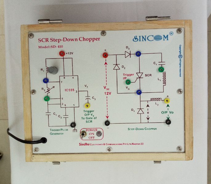
 Trainer SB-412")
This has Built-In DC +12V/ AC 12V 50Hz/500mA Fixed Power supply, SCR 2P4M / TYN604 with UJT as relaxation oscillator and resistive load is used to study all the SCR gate triggering methods like SCR gate triggering using DC Voltage, using AC Voltage, UJT relaxation oscillator, using Square wave I/P, using RC Network (5 Methods), maximum test points provided to observe the intermediate effects.
Objectives :
Accessories Included : Set of Patch Cords, Operating Manual.
 Trainer SB-913")
This has Built-In DC ±12V/1A regulated fixed Power supply, variable ±12V Power supply, Potential divider network to provide V1-V4 DC input levels, Two Op-Amps IC 741 with Open terminals for interconnection with RC components bank provided on the board to study following applications of Op-Amp IC741, fixed and variable Resistor bank (17 Nos), fixed capacitors bank (4Nos), detailed instruction manual with circuit diagram and procedure to determine all 16 parameters of given Op-Amp.
Objectives :
Accessories Included : Set of Patch Cords, Operating Manual.

This has Built-In DC +12V/1A regulated fixed Power supply, variable +12V Power supply, One Timer IC 555 with Open terminals for interconnection with RC components are provided on the board to study configure the various applications of Timer IC555, fixed Resistor bank (9Nos), variable Resistor/Potentiometers bank of 10K, 100K, 1M (3Nos), fixed capacitors bank (8Nos), Diode 1N4007, LED, relay, NPN Transistor, Speaker, detailed instruction manual with circuit diagram and procedure to study applications.
Objectives :
Accessories Included : Set of Patch Cords, Operating Manual.
 SE-604")
Product Category : Electrical Network Circuits and Bridges Lab Trainer (Series : 600)
Product Name : Kirchoff’s Laws (KCL & KVL)
Model No. : SE-604
Product Details :

Product Category : Electrical Network Circuits and Bridges Lab Trainer (Series : 600)
Product Name : Thevenin’s Theorem
Model No. : SE-619
Product Details

Product Category : Electrical Network Circuits and Bridges Lab Trainer (Series : 600)
Product Name : Superposition Theorem
Model No. : SE-622
Product Details

Product Category : Electrical Network Circuits and Bridges Lab Trainer (Series : 600)
Product Name : Maxwell’s Bridge
Model No.: SE-635
Product Details :

Product Category : Electronics Measuring Instruments Demonstrator (Series : 800)
Product Name : Digital Frequency Counter Demonstrator
Model No. : SE-805
Product Details :

Product Category : Electronics Measuring Instruments Demonstrator (Series : 800)
Product Name : Signal Generator Demonstrator
Model No. : SE-806
Product Details :
 SB-901")
Product Category : Electronics Measuring Instruments Demonstrator (Series : 800)
Product Name : DC Power Supply Demonstrator with faults creating facility (Single 0-30V/2A)
Model No.: SB-901
Product Details :

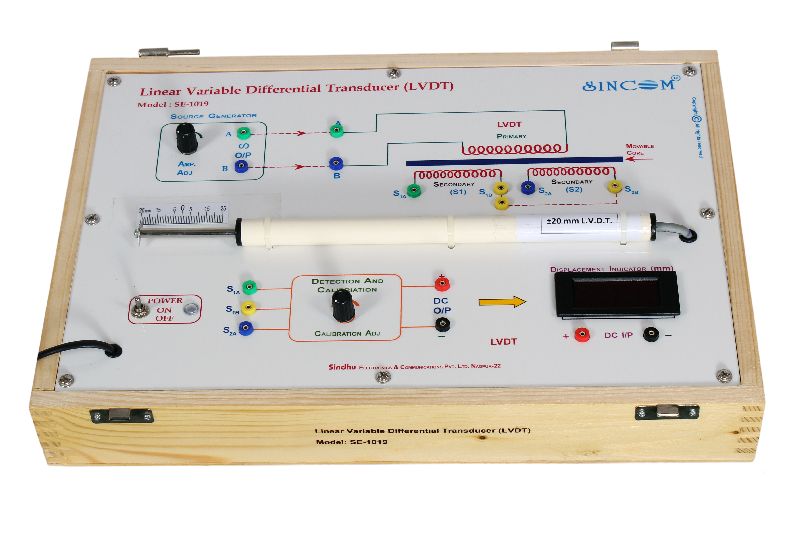
Product Category : Instrumentation and Control System Lab Trainer (Series: 1000)
Product Name : P, PI, PID Control System- Temperature control
Model No.: SE-1027
Product Details

Product Category : Digital Communication Lab Trainer (Series : 200-B)
Product Name : Adaptive Delta Modulation & Demodulation
Model No. : SB-212
Product Details :