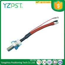
Company Information
Ask for more detail from the seller
Contact SupplierSymbol | Parameter | Values | Units | Test Conditions |
Tj | Operating temperature | -40~125 | °C |
|
Tstg | Storage temperature | -40~150 | °C |
|
R th (j-c) | Thermal resistance - junction to case | 0.4 | °C/W | DC operation ,Single sided cooled |
R th (c-s) | Thermal resistance - case to sink | 0.08 | °C/W | Single sided cooled |
P | Mounting force | - | Nm |
|
W | Weight | - | g | about |
Maximum Ratings And Characteristics
Symbol | Parameter | Values | Units | Test Conditions | |
ON-STATE |
|
|
| ||
ITAV | Mean on-state current | - | A | Sinewave,180° conduction,Tc=100°C | |
ITRMS | RMS value of on-state current | 100 | A | Nominal value | |
ITSM | Peak one cycle surge (non repetitive) current | 900 | A | 10.0 msec (50Hz), sinusoidal wave- shape, 180o conduction, Tj = 125 °C | |
I2t | I square t | 4050 | A2s | 8.3 msec and 10.0 msec | |
IL | Latching current | 100 | mA | VD = 12 V; RL= 12 ohms | |
IH | Holding current | 30 | mA | VD = 12 V; I = 1 A | |
VTM | Peak on-state voltage | 2.0 | V | ITM = 150 A; Duty cycle £ 0.01%; Tj = 25 °C
| |
di/dt | Critical rate of rise of on-state current | non-repetitive | 300 | A/ms | Gate drive 20V, 20Ω, tr≤1μs, Tj=Tjmax, anode voltage≤80% VDRM |
repetitive | 50 | ||||
BLOCKING |
|
|
| ||
VDRM VRRM | Repetitive peak off state voltage Repetitive peak reverse voltage | 600 | V |
| |
VDSM VRSM | Non repetitive peak off state voltage Non repetitive peak reverse voltage | 700 | V |
| |
IDRM IRRM | Repetitive peak off state current Repetitive peak reverse current | 10 | mA | Tj = 125 °C ,VRRM VDRM applied | |
dV/dt | Critical rate of voltage rise | 100 | V/ms | TJ=TJmax, linear to 80% rated VDRM | |
TRIGGEING |
|
|
| ||
PG(AV) | Average gate power dissipation | - | W |
| |
PGM | Peak gate power dissipation | - | W |
| |
IGM | Peak gate current | - | A |
| |
IGT | Gate trigger current | 200 | mA | TC = 25 °C | |
VGT | Gate trigger voltage | 3.0 | V | TC = 25 °C | |
VT(T0) | Treshold voltage | 1 | V |
| |
rT | Slope resistance | 2.4 | mΩ |
| |
VGD | Gate non-trigger voltage | 0.2 | V | Tj = 125 °C | |
SWITCHING |
|
|
| ||
tq | Turn-off time | - | ms | Tj = 125 °C | |
td | Delay time | - | Gate current 1A, di/dt=1A/μs, Vd=0.67%VDRM, TJ=25 °C | ||
Qrr | Reverse recovery charge | - |
|
| |

