Products / Services
  • Products / Services
  • Companies
  • Buy Leads
    Post Buy Requirement

    Gallium Arsenide Wafer, Brand Name : GaAs substrate

    • Brand NameGaAs wafer, Gallium Arsenide wafer, GaAs substrate
    • Supply TypeManufacturer
    • Preferred Buyer Location All over the world

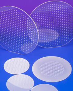
    We are offering gallium arsenide wafer. Pam develops and manufactures compound semiconductor substrates-gallium arsenide crystal and wafer.we has used advanced crystal growth technology,vertical gradient freeze(vgf) and gaas wafer processing technology,established a production line from crystal growth, cutting, grinding to polishing processing and built a 100-class clean room for wafer cleaning and packaging. Our gaas wafer include 2~6 inch ingotwafers for led,ld and microelectronics applications. Gaas epi wafer,gaas hemt,gaas mmic,gaas phemt,inp hemt epi wafer
    Send Enquiry

    Company Information

    • calendar Member Since 12 Years
    • building Nature of Business Manufacturer
    • Year of Establishment 1990

    Ask for more detail from the seller

    Contact Supplier
    Report incorrect details
    Share your requirements for a quick response!
    Tell us what you need?
    To list your productBoost Your Business Visibility WorldwideRegister Now
    Waiting for permission
    To search by voice, go to your browser settings and allow access to microphone

    Allow microphone access to search with voice