Company Information
Ask for more detail from the seller
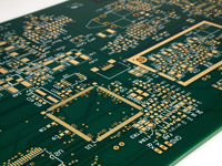
Contact SupplierCustom Manufacturing of Multilayer FR4 PCB for the Industrial Controls Industry
This 12 layer, FR4 printed circuit board (PCB), shown to the right, was custom manufactured by Standard Printed Circuit Boards for the industrial controls industry. The first step was to pull the proper laminates for innerlayer manufacture. Tooling holes were drilled in the panels and the order moved to the Imaging Department. Our skilled technicians utilized various Photolithographic methods to transfer the customer's design to the innerlayer panels and performed a thorough in-process inspection. Next the innerlayers moved into the Etching Department where all unwanted copper was chemically removed. Again, a thorough in-process inspection ensured that all specifications were met.
After receiving an oxide treatment, the innerlayers travelled into Lamination where layup of the panels took place. The hydraulic press was setup to laminate the panels at the proper pressure, temperature, and duration in order to create a high quality bond between all the layers. A cool down cycle took place before the panels moved into primary drilling.
Click to enlarge
Multilayer FR4
After primary drill, the panels were placed in our plasma etching unit where any residual drill smear was removed from the interior of the hole wall. This step helped to ensure the electrical integrity between the innerlayers and the plated holes. The panels then moved into our Direct Metalization Line where a conductive polymer was chemically bonded to the interior hole wall to facilitate subsequent copper electro-plating. After outer layer imaging, the panels were processed through the full build electrolytic copper line where a 1 mil minimum copper thickness was deposited on the hole walls and surface areas. A tin or tin-lead etch resist followed the copper process as the panels moved into the final etching process.
The boards were then coated with a liquid photoimageable (LPI) soldermask, baked thoroughly, and then moved into ENIG where a layer of gold was deposited over nickel on all the exposed copper surfaces and holes. The boards were then returned to the soldermask area to receive a silkscreened legend which will later assist in component placement during assembly. The boards then travelled in to Final Routing where CNC routers machined the boards to their final size and shape. The completed boards then proceeded to Final QA for inspection and Electrical Testing. 24 multilayer FR4 printed circuit boards were built for this client, vacuum packaging and delivery of all units to their facility in New York. The product met or exceeded both IPC-6012B and IPC-A-600 industry standards.

Connect with us