Products / Services
  • Products / Services
  • Companies
  • Buy Leads
    Post Buy Requirement

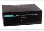
    PCB Design Fabrication Lab

    • MOQ1 Piece(s)
    • Development Tank Buzzer :For timer indication
    • Exposing area :20” x 10”
    • Dipping area :12” x 10”
    • Photo Resist Dip Coating Machine Dipping area :12” x 10”
    • Business TypeService Provider
    • Preferred Buyer Location All over the world
    View More Details
    Send Enquiry

    Company Information

    • calendar Member Since 9 Years
    • building Nature of Business Exporter
    • gst icon GST No. 23AAGCS1664P1ZZ

    Ask for more detail from the seller

    Contact Supplier
    Report incorrect details
    • Service Details

    • Company Details

    no_img_icon

    • Drill Machine Drill bits :0.8mm - 5 Nos., 1.0 mm - 5 Nos.
    • Photo Resist Dip Coating Machine Dipping area :12” x 10”
    • Artwork Table Supply :230V AC ± 10%, 50Hz
    • PCB Art Work Film Maker Supply :230V AC ± 10%, 50Hz
    • PCB Curing Machine Heating area :12” x 12”
    • PCB Etching Machine Motor :1/16 HP Pressure pump
    • Development Tank Buzzer :For timer indication
    • PCB Shearing Machine Mounting Base :Table Mounted / Floor Mounted
    • Light Exposed area :17” x 13”
    • UV Exposure Unit Exposing area :20” x 10”
    • Dye Tank Dipping area :12” x 10”
    • Dipping area :12” x 10”
    • Cutting Area :12”
    • Solderable Lacquer Tank Dipping area :12” x 10”
    • Exposing area :20” x 10”

    Nvis PCB LAB is a complete solution for designing PCB. This solution includes all the necessary machines and chemicals which are used in the PCB development process. The PCB artwork film maker is used as a contact printer for creating design films from the PCB Layout. The artwork table is used for manually designing the films and for correcting or changing the existing films. The shearing machine is used for cutting the PCB according to film size. The photoresist dip coating machine is used for coating photoresist on the PCB Laminate. After photoresist coating, the PCB and films are placed in UV exposure machine for exposing. After exposing the development tank is used to remove unused photoresist. The dye tank is used for highlighting the design on the PCB. The etching machine is used for removing unused copper from the PCB. The drilling machine is used for making the holes in the PCB. The PCB design kit is provided which include tapes, stencils and other accessories used for designing the PCB.


    Additional Information

    • Payment Terms T/T
    • Port of DispatchMumbai
    • Delivery Time6 Month
    Interested in this service? Ask for more details & Latest Price from service providers
    Send Enquiry
    Share your requirements for a quick response!
    Tell us what you need?

    Looking for PCB Design Fabrication Lab?

    Quantity
    Contact Details
    To list your productBoost Your Business Visibility WorldwideRegister Now
    To list your productBoost Your Business Visibility WorldwideRegister Now
    Waiting for permission
    To search by voice, go to your browser settings and allow access to microphone

    Allow microphone access to search with voice