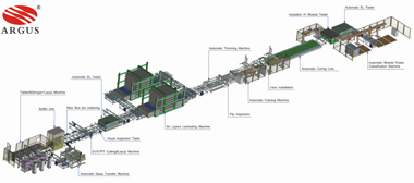
Our Product / Services
We offer the best product range of Bond Alignment Systems, Ingot Lifetime Scanning Machine, Ion Implantation Reactors, Panel Turnkey Line and Atomic Layer Deposition System.

EVG offers high precision, fully integrated and highly automated wafer Bond Aligner systems for bonding application such as anodic, silicon fusion, thermo-compression and eutectic bonding.
The alignment and bonding process separation results in higher flexibility and universal application of the wafer bonding equipment. The EVG bond alignment systems offer highest precision, flexibility, ease of use and modular upgrade capability and have been qualified in numerous high throughput production environments. The precision of EVG bond aligners accommodates most demanding alignment processes in MEMS production and in emerging fields like 3D integration applications.
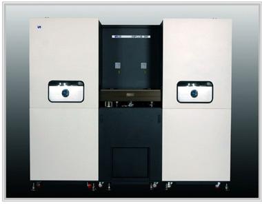
A maximum level of automation and process integration is achieved by the GEMINI Automated Production Wafer Bonding System. Wafer-to-wafer alignment and wafer bonding processes up to 200 mm (300 mm) for volume manufacturing are all performed in one fully automated platform. Device manufacturers benefit from increased production output, a high integration level and a big choice of process variations like anodic, silicon fusion, thermo-compression and eutectic bonding.
Ultra clean handling of wafers throughout the bonding process assures high-yield and void-free bonds. All essential steps, from cleaning and alignment to pre-bonding and IR-inspection are combined in one high volume production system. EVG850 is the only production bonding system built to operate in high throughput, high-yield environments and guarantees void-free SOI wafers up to 300 mm.

The LL 156/300 is designed to evaluate material quality quickly and economically. This handy machine helps to guarantee a steady quality of wafers
Mapping of carrier lifetime, photoconductivity, resistivityNon-contact, non-destructive electrical semiconductor characterisationTwo dimensional ingot mapping system for solar grade multi siliconMeasurement time: 2 minutes for two surfaces simultaneouslyOne ingot four sides with handling: 5 6 minResolution 1 mm