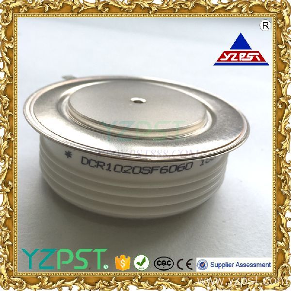
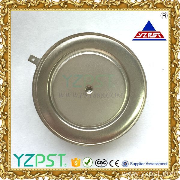
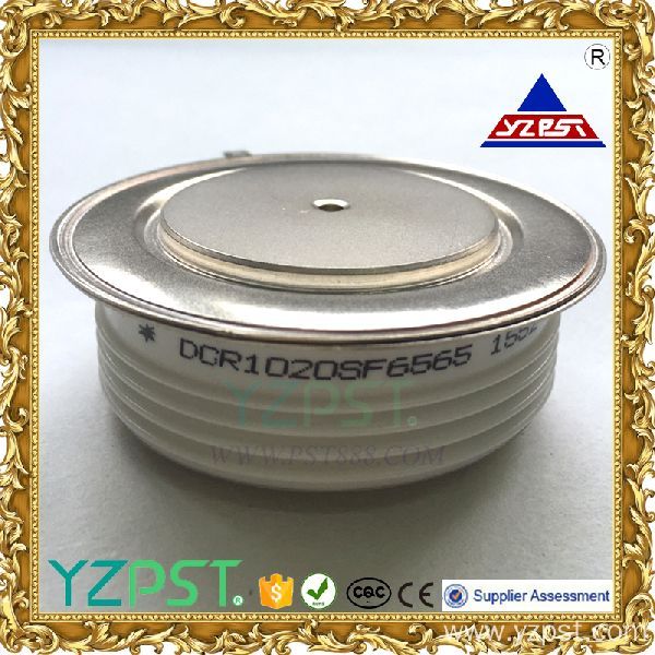
Our Products
We offer the best product range of Gate Turn off Thyristor, 165A Inverter Thyristor, DCR1020 Phase Control Power Thyristor, KK1000A Fast KK Converter Thyristor and Phase Control Thyristor 400a.

Additional Information:
Payment Terms : L/C, T/T,
Delivery Time : 30 Days

Additional Information:
Payment Terms : L/C, T/T,
Delivery Time : 30 Days
Additional Information:
Payment Terms : L/C, T/T,
Delivery Time : 30 Days

Additional Information:
Payment Terms : L/C, T/T,
Delivery Time : 30 Days
Detail 01
|
Critical rate of rise of on-state current (5, 6) |
di/dt |
|
800 |
|
A/ms |
Switching from VDRM£ 1000 V, non-repetitive |
|---|---|---|---|---|---|---|
|
Critical rate of rise of on-state current (6) |
di/dt |
|
200 |
|
A/ms |
Switching from VDRM£ 1000 V |
Detail 02
|
Parameter |
Symbol |
Min. |
Max. |
Typ. |
Units |
Conditions |
|---|---|---|---|---|---|---|
|
Average value of on-state current |
IT(AV) |
|
1000 |
|
A |
Sinewave,180o conduction,Tc=80oC |
|
RMS value of on-state current |
ITRMS |
|
1570 |
|
A |
Nominal value |
|
Peak one cPSTCle surge (non repetitive) current |
ITSM |
|
-
18500 |
|
A
A |
8.3 msec (60Hz), sinusoidal wave- shape, 180o conduction, Tj = 125 oC 10.0 msec (50Hz), sinusoidal wave- shape, 180o conduction, Tj = 125 oC |
|
I square t |
I2t |
|
1.66x10⁶ |
|
A2s |
8.3 msec and 10.0 msec |
|
Latching current |
IL |
|
- |
|
mA |
VD = 24 V; RL= 12 ohms |
|
Holding current |
IH |
|
- |
|
mA |
VD = 24 V; I = 2.5 A |
|
Peak on-state voltage |
VTM |
|
1.45 |
|
V |
ITM = 1000 A; Duty Cycle £ 0.01%; Tj =1 25 oC |
Gating
|
Parameter |
Symbol |
Min. |
Max. |
Typ. |
Units |
Conditions |
|---|---|---|---|---|---|---|
|
Peak gate power dissipation |
PGM |
|
100 |
|
W |
tp = 40 us |
|
Average gate power dissipation |
PG(AV) |
|
5 |
|
W |
|
|
Peak gate current |
IGM |
|
- |
|
A |
|
|
Gate current required to trigger all units |
IGT |
|
- 120 - |
|
mA mA mA |
VD = 6 V;RL = 3 ohms;Tj = -40 oC VD = 6 V;RL = 3 ohms;Tj = +25 oC VD = 6 V;RL = 3 ohms;Tj = +125oC |
|
Gate voltage required to trigger all units
|
VGT |
|
- 3.0 -
|
|
V V V |
VD = 6 V;RL = 3 ohms;Tj = -40 oC VD = 6 V;RL = 3 ohms;Tj = 0-125oC VD = Rated VDRM; RL = 1000 ohms;Tj = + 125 oC |
|
Peak negative voltage |
VGRM |
|
20 |
|
V |
|
Dynamic
|
Parameter |
Symbol |
Min. |
Max. |
Typ. |
Units |
Conditions |
|
Delay time |
td |
|
- |
0.7 |
ms |
ITM = 50 A; VD = Rated VDRM Gate pulse: VG = 20 V; RG = 20 ohms; tr = 0.1 ms; tp = 20 ms |
|
Turn-off time (with VR = -50 V) |
tq |
|
- |
50 |
ms |
ITM = 1000 A; di/dt = 25 A/ms; VR³ -50 V; Re-applied dV/dt = 20 V/ms linear to 80% VDRM; VG = 0;Tj = 125 oC; Duty cPSTCle ³ 0.01% |
|
Reverse recovery charge |
Qrr |
|
* |
|
mC |
ITM = 1000 A; di/dt = 25 A/ms; VR³ -50 V |
THERMAL AND MECHANICAL CHARACTERISTICS AND RATINGS
|
Parameter |
Symbol |
Min. |
Max. |
Typ. |
Units |
Conditions |
|---|---|---|---|---|---|---|
|
Operating temperature |
Tj |
-40 |
+125 |
|
oC |
|
|
Storage temperature |
Tstg |
-40 |
+125 |
|
oC |
|
|
Thermal resistance - junction to case |
RQ (j-c) |
|
0.023 - |
|
oC/W |
Double sided cooled Single sided cooled |
|
Thermal resistamce - case to sink |
RQ (c-s) |
|
0.0075 - |
|
oC/W |
Double sided cooled * Single sided cooled * |
|
Mounting force |
P |
22.2 |
26.6 |
|
kN |
|
|---|---|---|---|---|---|---|
|
Weight |
W |
|
|
- |
g |
About |

Additional Information:
Payment Terms : L/C, D/P, T/T
Delivery Time : 30 Days
|
Thyristor |
Ratings |
||||||
|
Symbol |
Definition |
Conditions |
|
min. |
typ. |
max. |
Unit |
|
V EQ \F(RSM,DSM) |
max. non-repetitive reverse/forward blocking voltage |
TJ = 25°C |
|
|
1900 |
V |
|
|
V EQ \F(RRM,DRM) |
max. repetitive reverse/forward blocking voltage |
TJ = 25°C |
|
|
1800 |
V |
|
|
VT |
On-state voltage |
IT=1100 A |
TJ = 25°C |
|
|
1.85 |
V |
|
IT(AV) |
average forward current |
TC=25°C |
|
|
|
400 |
A |
|
IT(RMS) |
RMS forward current |
180° sine |
|
|
|
530 |
A |
|
RthJC |
thermal resistance junction to case |
|
|
|
|
|
K/W |
|
RthCH |
thermal resistance case to heatsink |
|
|
|
|
|
K/W |
|
RthJK |
thermal resistance junction to heatsink |
|
|
|
|
0.048 |
K/W |
|
ITSM |
max. forward surge current |
t = 10 ms; (50 Hz), sine |
TJ = 25°C |
|
|
6.3 |
kA |
|
I²t |
value for fusing |
t = 10 ms; (50 Hz), sine |
TJ = 25°C |
|
|
198 |
kA²s |
|
di/dt |
Rate of rise of on-state current |
TJ = 125°C; f = 50 Hz tP=200µs;diG/dt=0.15A/µs; IG=0.15A;VD= â��VDRM |
repetitive |
|
|
160 |
A/µs |
|
non-repet |
|
|
320 |
A/µs |
|||
|
dv/dt |
Maximum linear rate of rise of off-state voltage |
VD= â��VDRM RGK =∞; method 1 (linear voltage rise) |
TJ = 125°C |
|
|
1000 |
V/µs |
|
VGT |
gate trigger voltage |
VD = 6V |
TJ = 25°C |
|
|
2.5 |
V |
|
IGT |
gate trigger current |
VD = 6V |
TJ = 25°C |
|
|
250 |
mA |
|
IL |
latching current |
|
TJ = 25°C |
|
|
|
A |
|
IH |
holding current |
|
TJ = 25°C |
|
|
300 |
mA |
|
tgd |
gate controlled delay time |
|
TJ = 25°C |
|
|
2.5 |
µs |
|
tq |
Turn-off time |
VR=10 V; IT=20A; VD=�VDRM |
TJ = 150°C |
|
200 |
400 |
µs |
|
Tstg |
storage temperature |
|
|
-60 |
|
125 |
°C |
|
TJ |
virtual junction temperature |
|
|
-60 |
|
120 |
°C |
|
Wt |
Weight |
|
|
|
|
|
g |
|
F |
mounting force |
|
|
9 |
|
11 |
kN |

Additional Information:
Payment Terms : L/C, T/T,
Delivery Time : 30 Days
Detail 01
|
VRRM (1) |
VDRM (1) |
VRSM (1) |
|---|---|---|
|
1200 |
1200 |
1300 |
|
Repetitive peak reverse leakage and off state leakage |
IRRM / IDRM |
20 mA 150mA (3) |
|---|---|---|
|
Critical rate of voltage rise |
dV/dt (4) |
200 V/msec |
Detail 02
Conducting - on state
|
Parameter |
Symbol |
Min. |
Max. |
Typ. |
Units |
Conditions |
|
Max. average value of on-state current |
IT(AV)M |
|
1271 |
|
A |
Sinewave,180o conduction,Tc=55oC |
|
RMS value of on-state current |
IT(RMS)m |
|
2599 |
|
A |
Nominal value |
|
Peak one cPSTCle surge (non repetitive) current |
ITSM |
|
-
18.0 |
|
kA
kA |
8.3 msec (60Hz), sinusoidal wave- shape, 180o conduction, Tj = 125 oC 10.0 msec (50Hz), sinusoidal wave- shape, 180o conduction, Tj = 125 oC |
|
I square t |
I2t |
|
1.62x10⁶ |
|
A2s |
8.3 msec |
|
Latching current |
IL |
|
- |
|
mA |
VD = 24 V; RL= 12 ohms |
|
Holding current |
IH |
|
1000 |
|
mA |
VD = 24 V; I = 2.5 A |
|
Peak on-state voltage |
VTM |
|
2.02 |
|
V |
ITM = 2000 A |
|
Critical rate of rise of on-state current (5, 6) |
di/dt |
|
1500 |
|
A/ms |
Switching from VDRM £ 1000 V, non-repetitive |
|
Critical rate of rise of on-state current (6) |
di/dt |
|
1000 |
|
A/ms |
Switching from VDRM £ 1000 V |
Gating
|
Parameter |
Symbol |
Min. |
Max. |
Typ. |
Units |
Conditions |
|---|---|---|---|---|---|---|
|
Peak gate power dissipation |
PGM |
|
30 |
|
W |
|
|
Average gate power dissipation |
PG(AV) |
|
2 |
|
W |
|
|
Peak gate current |
IGM |
|
- |
|
A |
|
|
Gate current required to trigger all units |
IGT |
|
300 |
|
mA |
VD = 10 V;IT=3A;Tj = +25 oC
|
|
Gate voltage required to trigger all units
|
VGT |
|
3.0 |
|
V
|
VD = 10 V;IT=3A;Tj = +25 oC
|
|
Peak negative voltage |
VRGM |
|
5 |
|
V |
|
Dynamic
|
Parameter |
Symbol |
Min. |
Max. |
Typ. |
Units |
Conditions |
|---|---|---|---|---|---|---|
|
Delay time |
tgd |
|
1.0 |
- |
ms |
VD=67% VDRM, IT=2000A, di/dt=60A/us, IFG=2A, tr=0.5us, Tj=25C |
|
Turn-on time |
tgt |
|
2.0 |
- |
|
|
|
Turn-off time (with VR = -5 V) |
tq |
- |
- |
15 |
ms |
ITM=1000A, tp=1000us, di/dt=60A/us, Vr=50V, Vdr=80%VDRM, dVdr/dt=20V/us |
|
Reverse recovery current |
Irm |
|
- |
|
A |
ITM=4000A, tp=2000us, di/dt=60A/us |
THERMAL AND MECHANICAL CHARACTERISTICS AND RATINGS
|
Parameter |
Symbol |
Min. |
Max. |
Typ. |
Units |
Conditions |
|---|---|---|---|---|---|---|
|
Operating temperature |
Tj |
-40 |
+125 |
|
oC |
|
|
Storage temperature |
Tstg |
-40 |
+150 |
|
oC |
|
|
Thermal resistance - junction to case |
RQ (j-c) |
|
- - |
|
K/kW |
Double sided cooled Single sided cooled |
|
Thermal resistamce - case to sink |
RQ (c-s) |
|
- - |
|
K/kW |
Double sided cooled * Single sided cooled * |
|
Thermal resistance - junction to case |
RQ (j-s) |
|
24 48 |
|
K/kW |
Double sided cooled Single sided cooled |
|
Mounting force |
F |
19 |
25 |
- |
kN |
|
|
Weight |
W |
|
|
- |
Kg |
about |

Additional Information:
Payment Terms : L/C, T/T,
Delivery Time : 30 Days
Details
|
Parameter |
Symbol |
Min. |
Max. |
Typ. |
Units |
Conditions |
|---|---|---|---|---|---|---|
|
Average value of on-state current |
IT(AV) |
|
1300 |
|
A |
Sinewave,180o conduction,Tc=65oC |
|
RMS value of on-state current |
ITRMS |
|
2000 |
|
A |
Nominal value |
|
Peak one cPSTCle surge (non repetitive) current |
ITSM |
|
20000
18000 |
|
A
A |
8.3 msec (60Hz), sinusoidal wave- shape, 180o conduction, Tj = 125 oC 10.0 msec (50Hz), sinusoidal wave- shape, 180o conduction, Tj = 125 oC |
|
I square t |
I2t |
|
1.7x10⁶ |
|
A2s |
8.3 msec and 10.0 msec |
|
Latching current |
IL |
|
800 |
|
mA |
VD = 24 V; RL= 12 ohms |
|
Holding current |
IH |
|
400 |
|
mA |
VD = 24 V; I = 2.5 A |
|
Peak on-state voltage |
VTM |
|
1.75 |
|
V |
ITM = 3000 A; Duty cPSTCle £ 0.01% |
|
Critical rate of rise of on-state current (5, 6) |
di/dt |
|
600 |
|
A/ms |
Switching from VDRM£ 1000 V, non-repetitive |
|
Critical rate of rise of on-state current (6) |
di/dt |
|
200 |
|
A/ms |
Switching from VDRM£ 1000 V |
ELECTRICAL CHARACTERISTICS AND RATINGS (cont`d)
Gating
|
Parameter |
Symbol |
Min. |
Max. |
Typ. |
Units |
Conditions |
|---|---|---|---|---|---|---|
|
Peak gate power dissipation |
PGM |
|
200 |
|
W |
tp = 40 us |
|
Average gate power dissipation |
PG(AV) |
|
5 |
|
W |
|
|
Peak gate current |
IGM |
|
10 |
|
A |
|
|
Gate current required to trigger all units |
IGT |
|
300 150 125 |
|
mA mA mA |
VD = 6 V;RL = 3 ohms;Tj = -40 oC VD = 6 V;RL = 3 ohms;Tj = +25 oC VD = 6 V;RL = 3 ohms;Tj = +125oC |
|
Gate voltage required to trigger all units
|
VGT |
0.30 |
5 3
|
|
V V V |
VD = 6 V;RL = 3 ohms;Tj = -40 oC VD = 6 V;RL = 3 ohms;Tj = 0-125oC VD = Rated VDRM; RL = 1000 ohms; Tj = + 125 oC |
|
Peak negative voltage |
VGRM |
|
5 |
|
V |
|
Dynamic
|
Parameter |
Symbol |
Min. |
Max. |
Typ. |
Units |
Conditions |
|---|---|---|---|---|---|---|
|
Delay time |
td |
|
1.5 |
0.7 |
ms |
ITM = 50 A; VD = Rated VDRM Gate pulse: VG = 20 V; RG = 20 ohms; tr = 0.1 ms; tp = 20 ms |
|
Turn-off time (with VR = -50 V) |
tq |
|
250 |
150 |
ms |
ITM = 1000 A; di/dt = 25 A/ms; VR³ -50 V; Re-applied dV/dt = 20 V/ms linear to 80% VDRM; VG = 0; Tj = 125 oC; Duty cPSTCle ³ 0.01% |
|
Reverse recovery charge |
Qrr |
|
* |
|
mC |
ITM = 1000 A; di/dt = 25 A/ms; VR³ -50 V |
* For guaranteed max. value, contact factory.
THERMAL AND MECHANICAL CHARACTERISTICS AND RATINGS
|
Parameter |
Symbol |
Min. |
Max. |
Typ. |
Units |
Conditions |
|---|---|---|---|---|---|---|
|
Operating temperature |
Tj |
-40 |
+125 |
|
oC |
|
|
Storage temperature |
Tstg |
-40 |
+150 |
|
oC |
|
|
Thermal resistance - junction to case |
RQ (j-c) |
|
0.025 0.050 |
|
oC/W |
Double sided cooled Single sided cooled |
|
Thermal resistamce - case to sink |
RQ (c-s) |
|
0.010 0.020 |
|
oC/W |
Double sided cooled * Single sided cooled * |
|
Mounting force |
P |
24.5 |
26.7 |
|
kN |
|
|
Weight |
W |
|
|
460 |
g |
|

Additional Information:
Payment Terms : L/C, T/T,
Delivery Time : 30 Days
Details
|
Parameter |
Symbol |
Min. |
Max. |
Typ. |
Units |
Conditions |
|---|---|---|---|---|---|---|
|
Average value of on-state current |
IT(AV) |
|
1275 |
|
A |
Tc=55oC |
|
RMS value of on-state current |
ITRMS |
|
1870 |
|
A |
Nominal value |
|
Peak one cPSTCle surge (non repetitive) current |
ITSM |
|
21400
18900 |
|
A
A |
8.3 msec (60Hz), sinusoidal wave- shape, 180o conduction, Tj = 125 oC 10.0 msec (50Hz), sinusoidal wave- shape, 180o conduction, Tj = 125 oC |
|
I square t |
I2t |
|
2.66x10⁶ |
|
A2s |
8.3 msec and 10.0 msec |
|
Latching current |
IL |
|
1000 |
|
mA |
VD = 24 V; RL= 12 ohms |
|
Holding current |
IH |
|
500 |
|
mA |
VD = 24 V; I = 2.5 A |
|
Peak on-state voltage |
VTM |
|
1.90 |
|
V |
ITM = 2000 A; Duty cPSTCle £ 0.01% |
|
Critical rate of rise of on-state current (5, 6) |
di/dt |
|
1000 |
|
A/ms |
Switching from VDRM£ 1000 V, non-repetitive |
Gating
|
Parameter |
Symbol |
Min. |
Max. |
Typ. |
Units |
Conditions |
|---|---|---|---|---|---|---|
|
Peak gate power dissipation |
PGM |
|
200 |
|
W |
tp = 40 us |
|
Average gate power dissipation |
PG(AV) |
|
5 |
|
W |
|
|
Peak gate current |
IGM |
|
10 |
|
A |
|
|
Gate current required to trigger all units |
IGT |
|
300 150 125 |
|
mA mA mA |
VD = 6 V;RL = 3 ohms;Tj = -40 oC VD = 6 V;RL = 3 ohms;Tj = +25 oC VD = 6 V;RL = 3 ohms;Tj = +125oC |
|
Gate voltage required to trigger all units
|
VGT |
0.30 |
5 3
|
|
V V V |
VD = 6 V;RL = 3 ohms;Tj = -40 oC VD = 6 V;RL = 3 ohms;Tj = 0-125oC VD = Rated VDRM; RL = 1000 ohms; Tj = + 125 oC |
|
Peak negative voltage |
VGRM |
|
5 |
|
V |
|
Dynamic
|
Parameter |
Symbol |
Min. |
Max. |
Typ. |
Units |
Conditions |
|---|---|---|---|---|---|---|
|
Delay time |
td |
|
1.5 |
0.7 |
ms |
ITM = 500 A; VD = Rated VDRM Gate pulse: VG = 20 V; RG = 20 ohms; tr = 0.1 ms; tp = 20 ms |
|
Turn-off time (with VR = -50 V) |
tq |
|
40
|
|
ms |
ITM = 1000 A; di/dt = 25 A/ms;VR³ -50 V; Re-applied dV/dt = 200 V/ms linear to 80% VDRM; VG = 0; Tj = 125 oC; Duty cPSTCle ³ 0.01% |
|
Reverse recovery charge |
Qrr |
|
* |
2000 |
mC |
ITM = 1000 A; di/dt = 25 A/ms;VR³ -50 V |
* For guaranteed max. value, contact factory.
THERMAL AND MECHANICAL CHARACTERISTICS AND RATINGS
|
Parameter |
Symbol |
Min. |
Max. |
Typ. |
Units |
Conditions |
|---|---|---|---|---|---|---|
|
Operating temperature |
Tj |
-40 |
+125 |
|
oC |
|
|
Storage temperature |
Tstg |
-40 |
+150 |
|
oC |
|
|
Thermal resistance - junction to case |
RQ (j-c) |
|
0.023 0.046 |
|
oC/W |
Double sided cooled Single sided cooled |
|
Thermal resistamce - case to sink |
RQ (j-c) |
|
0.010 0.020 |
|
oC/W |
Double sided cooled * Single sided cooled * |
|
Mounting force |
P |
19.5 |
21 |
|
kN |
|

Additional Information:
Payment Terms : L/C, T/T,
Delivery Time : 30 Days
|
VRRM (1) |
VDRM (1) |
VRSM (1) |
|
15 |
1000 |
15 |
|
Repetitive peak reverse leakage and off state leakage |
IRRM / IDRM
|
5 mA 40 mA (3) |
|
Critical rate of voltage rise (4) |
dV/dt |
1000 V/msec |
Conducting - on state
|
Parameter |
Symbol |
Min. |
Max. |
Typ. |
Units |
Conditions |
|
Average value of on-state current |
IT(AV) |
|
438 |
|
A |
Sinewave,180o conduction,Tc =85oC |
|
RMS value of on-state current |
ITRMS |
|
900 |
|
A |
Nominal value |
|
Peak one cycle surge (non repetitive) current |
ITSM |
|
-
5500 |
|
A
A |
8.3 msec (60Hz), sinusoidal wave- shape, 180o conduction, Tj = 125 oC 10.0 msec (50Hz), sinusoidal wave- shape, 180o conduction, Tj = 125 oC |
|
I square t |
I2t |
|
1.5 |
|
KA2s |
8.3 msec and 10.0 msec |
|
Latching current |
IL |
|
- |
|
mA |
VD = 24 V; RL= 12 ohms |
|
Holding current |
IH |
|
1000 |
|
mA |
VD = 24 V; I =2.5 A |
|
Peak on-state voltage |
VTM |
|
2.1 |
|
V |
ITM = 1500 A; Duty cycle £ 0.01%
|
|
Critical rate of rise of on-state current (5, 6) |
di/dt |
|
- |
|
A/ms |
Switching from VDRM £ 1000 V, non-repetitive |
|
Critical rate of rise of on-state current (6) |
di/dt |
|
500 |
|
A/ms |
Switching from VDRM £ 1000 V |
ELECTRICAL CHARACTERISTICS AND RATINGS
Gating
|
Parameter |
Symbol |
Min. |
Max. |
Typ. |
Units |
Conditions |
|
Peak gate power dissipation |
PGM |
|
30 |
|
W |
tp = 40 us |
|
Average gate power dissipation |
PG(AV) |
|
10 |
|
W |
|
|
Peak gate current |
IGM |
|
- |
|
A |
|
|
Gate current required to trigger all units |
IGT |
|
300
|
|
mA mA mA |
VD = 6 V;RL = 3 ohms;Tj = -40 oC VD = 6 V;RL = 3 ohms;Tj = +25 oC VD = 6 V;RL = 3 ohms;Tj = +125oC |
|
Gate voltage required to trigger all units
|
VGT |
|
- 2.7
|
|
V V V |
VD = 6 V;RL = 3 ohms;Tj = -40 oC VD = 6 V;RL = 3 ohms;Tj = 0-125oC VD = Rated VDRM; RL = 1000 ohms; Tj = + 125 oC |
|
Peak negative voltage |
VGRM |
|
- |
|
V |
|
Dynamic
|
Parameter |
Symbol |
Min. |
Max. |
Typ. |
Units |
Conditions |
|
Delay time |
td |
|
|
1 |
ms |
ITM =50 A; VD = Rated VDRM Gate pulse: VG = 20 V; RG = 20 ohms; tr= 0.1 ms; tp = 20 ms |
|
Turn-off time (with VR = -50 V) |
tq |
- |
- |
15 |
ms |
ITM =500 A; di/dt =25 A/ms; VR ³ -50 V; Re-applied dV/dt = 20 V/ms linear to 80% VDRM; VG = 0; Tj = 125 oC; Duty cPSTCle ³ 0.01% |
|
Reverse recovery charge |
Qrr |
|
* |
|
mC |
ITM =500 A; di/dt =25 A/ms; VR ³ -50 V |
* For guaranteed max. value, contact factory.
THERMAL AND MECHANICAL CHARACTERISTICS AND RATINGS
|
Parameter |
Symbol |
Min. |
Max. |
Typ. |
Units |
Conditions |
|
Operating temperature |
Tj |
-40 |
+125 |
|
oC |
|
|
Storage temperature |
Tstg |
-40 |
+150 |
|
oC |
|
|
Thermal resistance - junction to case |
RQ (j-c)
|
|
|
53 - |
oC/KW |
Double sided cooled * Single sided cooled * |
|
Thermal resistamce - case to sink |
RQ (c-s) |
|
|
- - |
oC/KW |
Double sided cooled * Single sided cooled * |
|
Thermal resistance - junction to sink |
RQ (j-s) |
|
|
- - |
oC/KW |
Double sided cooled * Single sided cooled * |
|
Mounting force |
P |
5 |
9 |
- |
kN |
|
|
Weight |
W |
|
|
- |
g |

Additional Information:
Payment Terms : L/C, T/T,
Delivery Time : 30 Days
Details
|
Symbol |
Condition |
Ratings |
Unit |
|
IT(AV) |
Single phase,half wave,180° conduction ;TC=85°C |
800 |
A |
|
ITRMS |
Single phase,half wave,180° conduction |
1372 |
A |
|
ITSM |
Tj=125°C |
18.9 |
kA |
|
I2t |
Tj=125°C |
1.79×10³ |
kA2S |
|
VDRM/VRRM |
Tj=125°C |
1600/1600 |
V |
|
di/dt |
non-repetitive |
400 |
A/us |
|
Viso |
A.C.1minute |
3000 |
V |
|
Tj |
|
-40 ~ + 125 |
°C |
|
Tstg |
|
-40 ~ + 125 |
°C |
|
W |
About |
2.1 |
Kg |
Electrical Characteristics
|
Symbol |
Condition |
Ratings |
Unit |
|
IDRM /IRRM |
AtVDRM,Single phase,half wave,Tj=125°C |
100 |
mA |
|
VTM |
On-State Current 2400A,Tj=125°C |
1.52 |
V |
|
VT(TO) |
Tj=125°C |
0.93 |
V |
|
RK1G1 |
|
- |
Ω |
|
RK2G2 |
|
- |
Ω |
|
tgd |
Tj=25°C;VD=0.4VDRM;ITM=ITAV |
2.5 |
us |
|
tq |
dvD/dt=50V/us;Tj=125°C; ITM=ITAV |
320 |
us |
|
IGT/VGT |
Tj=25°C,IT=1A,VD=6V |
250 / 2.5 |
mA/V |
|
VGD |
VD=67%VDRM |
0.25 |
V |
|
DV/DT |
VD=67%VDRM |
1000 |
V/us |
|
IH |
Tj=25°C |
300 |
mA |
|
IL |
Tj=25°C |
- |
mA |
|
Rth(j-c) |
Per Module |
0.025 |
K/kW |

Additional Information:
Payment Terms : L/C, T/T,
Delivery Time : 30 Days
Details
|
Symbol |
Parameter |
Values |
Units |
Test Conditions |
|
|
ON-STATE |
|
|
|
||
|
ITAV |
Mean on-state current |
350 |
A |
Sinewave,180° conduction,Tc=85 |
|
|
ITRMS |
RMS value of on-state current |
550 |
A |
Nominal value |
|
|
ITSM |
Peak one cycle surge (non repetitive) current |
9.1 |
KA |
10.0 msec (50Hz), sinusoidal wave- shape, 180o conduction, Tj = 125 oC |
|
|
I2t |
I square t |
416 |
KA2s |
8.3 msec and 10.0 msec |
|
|
IL |
Latching current |
- |
mA |
VD = 24 V; RL= 12 ohms |
|
|
IH |
Holding current |
- |
mA |
VD = 24 V; I = 2.5 A |
|
|
VTM |
Peak on-state voltage |
1.4 |
V |
ITM = 625 A; Duty cycle £ 0.01%
|
|
|
di/dt |
Critical rate of rise of on-state current |
non-repetitive |
800 |
A/ms |
Gate drive 20V, 20Ω, tr≤1μs, Tj=Tjmax, anode voltage≤80% VDRM |
|
repetitive |
150 |
||||
|
BLOCKING |
|
|
|
||
|
VDRM VRRM |
Repetitive peak off state voltage Repetitive peak reverse voltage |
1200 |
V |
|
|
|
VDSM VRSM |
Non repetitive peak off state voltage Non repetitive peak reverse voltage |
1300 |
V |
|
|
|
IDRM IRRM |
Repetitive peak off state current Repetitive peak reverse current |
30 |
mA |
Tj = 125 oC ,VRRM VDRM applied |
|
|
dV/dt |
Critical rate of voltage rise |
1000 |
V/ms |
TJ=TJmax, linear to 80% rated VDRM |
|
|
TRIGGEING |
|
|
|
||
|
PG(AV) |
Average gate power dissipation |
3 |
W |
|
|
|
PGM |
Peak gate power dissipation |
16 |
W |
|
|
|
IGM |
Peak gate current |
- |
A |
|
|
|
IGT |
Gate trigger current |
150 |
mA |
TC = 25 oC |
|
|
VGT |
Gate trigger voltage |
3.0 |
V |
TC = 25 oC |
|
|
VGD |
Gate non-trigger voltage |
0.15 |
V |
Tj = 125 oC |
|
|
SWITCHING |
|
|
|
||
|
tq |
Turn-off time |
150 |
ms |
ITM=550A, TJ=TJmax, di/dt=40A/μs, VR=50V, dv/dt=20V/μs, Gate 0V 100Ω, tp=500μs |
|
|
td |
Delay time |
- |
|
Gate current A, di/dt=40A/μs, Vd=0.67%VDRM, TJ=25 oC |
|
Qrr |
Reverse recovery charge |
- |
|
|
Thermal And Mechanical
|
Symbol |
Parameter |
Values |
Units |
Test Conditions |
|
Tj |
Operating temperature |
-40~125 |
oC |
|
|
Tstg |
Storage temperature |
-40~150 |
oC |
|
|
R th (j-c) |
Thermal resistance - junction to case |
0.1 |
oC/W |
DC operation ,Single sided cooled |
|
R th (c-s) |
Thermal resistance - case to sink |
0.05 |
oC/W |
Single sided cooled |
|
P |
Mounting force |
3.5 |
Nm |
|
|
W |
Weight |
- |
g |
about |

Additional Information:
Payment Terms : L/C, T/T,
Delivery Time : 30 Days
Detail 01
|
Symbol |
Parameter |
Values |
Units |
Test Conditions |
|
Tj |
Operating temperature |
-40~125 |
°C |
|
|
Tstg |
Storage temperature |
-40~150 |
°C |
|
|
R th (j-c) |
Thermal resistance - junction to case |
0.4 |
°C/W |
DC operation ,Single sided cooled |
|
R th (c-s) |
Thermal resistance - case to sink |
0.08 |
°C/W |
Single sided cooled |
|
P |
Mounting force |
- |
Nm |
|
|
W |
Weight |
- |
g |
about |
Detail 02
Maximum Ratings And Characteristics
|
Symbol |
Parameter |
Values |
Units |
Test Conditions |
|
|
ON-STATE |
|
|
|
||
|
ITAV |
Mean on-state current |
- |
A |
Sinewave,180° conduction,Tc=100°C |
|
|
ITRMS |
RMS value of on-state current |
100 |
A |
Nominal value |
|
|
ITSM |
Peak one cycle surge (non repetitive) current |
900 |
A |
10.0 msec (50Hz), sinusoidal wave- shape, 180o conduction, Tj = 125 °C |
|
|
I2t |
I square t |
4050 |
A2s |
8.3 msec and 10.0 msec |
|
|
IL |
Latching current |
100 |
mA |
VD = 12 V; RL= 12 ohms |
|
|
IH |
Holding current |
30 |
mA |
VD = 12 V; I = 1 A |
|
|
VTM |
Peak on-state voltage |
2.0 |
V |
ITM = 150 A; Duty cycle £ 0.01%; Tj = 25 °C
|
|
|
di/dt |
Critical rate of rise of on-state current |
non-repetitive |
300 |
A/ms |
Gate drive 20V, 20Ω, tr≤1μs, Tj=Tjmax, anode voltage≤80% VDRM |
|
repetitive |
50 |
||||
|
BLOCKING |
|
|
|
||
|
VDRM VRRM |
Repetitive peak off state voltage Repetitive peak reverse voltage |
600 |
V |
|
|
|
VDSM VRSM |
Non repetitive peak off state voltage Non repetitive peak reverse voltage |
700 |
V |
|
|
|
IDRM IRRM |
Repetitive peak off state current Repetitive peak reverse current |
10 |
mA |
Tj = 125 °C ,VRRM VDRM applied |
|
|
dV/dt |
Critical rate of voltage rise |
100 |
V/ms |
TJ=TJmax, linear to 80% rated VDRM |
|
|
TRIGGEING |
|
|
|
||
|
PG(AV) |
Average gate power dissipation |
- |
W |
|
|
|
PGM |
Peak gate power dissipation |
- |
W |
|
|
|
IGM |
Peak gate current |
- |
A |
|
|
|
IGT |
Gate trigger current |
200 |
mA |
TC = 25 °C |
|
|
VGT |
Gate trigger voltage |
3.0 |
V |
TC = 25 °C |
|
|
VT(T0) |
Treshold voltage |
1 |
V |
|
|
|
rT |
Slope resistance |
2.4 |
mΩ |
|
|
|
VGD |
Gate non-trigger voltage |
0.2 |
V |
Tj = 125 °C |
|
|
SWITCHING |
|
|
|
||
|
tq |
Turn-off time |
- |
ms |
Tj = 125 °C |
|
|
td |
Delay time |
- |
Gate current 1A, di/dt=1A/μs, Vd=0.67%VDRM, TJ=25 °C |
||
|
Qrr |
Reverse recovery charge |
- |
|
|
|

Additional Information:
Payment Terms : L/C, T/T,
Delivery Time : 30 Days

Additional Information:
Payment Terms : L/C, T/T,
Delivery Time : 30 Days
|
VRRM (1) |
VDRM (1) |
VRSM (1) |
|
10 |
2400/2800 |
10 |
|
Repetitive peak reverse leakage and off state leakage |
IRRM / IDRM
|
5 mA 40 mA (3) |
|
Critical rate of voltage rise (4) |
dV/dt |
1000 V/msec |
|
Parameter |
Symbol |
Min. |
Max. |
Typ. |
Units |
Conditions |
|
Average value of on-state current |
IT(AV) |
|
341 |
|
A |
Sinewave,180o conduction,Tc =85oC |
|
RMS value of on-state current |
ITRMS |
|
1040 |
|
A |
Nominal value |
|
Peak one cycle surge (non repetitive) current |
ITSM |
|
-
5700 |
|
A
A |
8.3 msec (60Hz), sinusoidal wave- shape, 180o conduction, Tj = 125 oC 10.0 msec (50Hz), sinusoidal wave- shape, 180o conduction, Tj = 125 oC |
|
I square t |
I2t |
|
1.5 |
|
KA2s |
8.3 msec and 10.0 msec |
|
Latching current |
IL |
|
- |
|
mA |
VD = 24 V; RL= 12 ohms |
|
Holding current |
IH |
|
1000 |
|
mA |
VD = 24 V; I =2.5 A |
|
Peak on-state voltage |
VTM |
|
2.45 |
|
V |
ITM = 1000 A; Duty cycle £ 0.01%
|
|
Critical rate of rise of on-state current (5, 6) |
di/dt |
|
2000 |
|
A/ms |
Switching from VDRM £ 1000 V, non-repetitive |
|
Critical rate of rise of on-state current (6) |
di/dt |
|
1000 |
|
A/ms |
Switching from VDRM £ 1000 V |
ELECTRICAL CHARACTERISTICS AND RATINGS
Gating
|
Parameter |
Symbol |
Min. |
Max. |
Typ. |
Units |
Conditions |
|
Peak gate power dissipation |
PGM |
|
30 |
|
W |
tp = 40 us |
|
Average gate power dissipation |
PG(AV) |
|
10 |
|
W |
|
|
Peak gate current |
IGM |
|
- |
|
A |
|
|
Gate current required to trigger all units |
IGT |
|
400
|
|
mA mA mA |
VD = 6 V;RL = 3 ohms;Tj = -40 oC VD = 6 V;RL = 3 ohms;Tj = +25 oC VD = 6 V;RL = 3 ohms;Tj = +125oC |
|
Gate voltage required to trigger all units
|
VGT |
|
- 3
|
|
V V V |
VD = 6 V;RL = 3 ohms;Tj = -40 oC VD = 6 V;RL = 3 ohms;Tj = 0-125oC VD = Rated VDRM; RL = 1000 ohms; Tj = + 125 oC |
|
Peak negative voltage |
VGRM |
|
- |
|
V |
|
Dynamic
|
Parameter |
Symbol |
Min. |
Max. |
Typ. |
Units |
Conditions |
|
Delay time |
td |
|
|
1 |
ms |
ITM =50 A; VD = Rated VDRM Gate pulse: VG = 20 V; RG = 20 ohms; tr= 0.1 ms; tp = 20 ms |
|
Turn-off time (with VR = -50 V) |
tq |
- |
- |
55 |
ms |
ITM =500 A; di/dt =25 A/ms; VR ³ -50 V; Re-applied dV/dt = 20 V/ms linear to 80% VDRM; VG = 0; Tj = 125 oC; Duty cPSTCle ³ 0.01% |
|
Reverse recovery charge |
Qrr |
|
* |
|
mC |
ITM =500 A; di/dt =25 A/ms; VR ³ -50 V |
* For guaranteed max. value, contact factory.
THERMAL AND MECHANICAL CHARACTERISTICS AND RATINGS
|
Parameter |
Symbol |
Min. |
Max. |
Typ. |
Units |
Conditions |
|
Operating temperature |
Tj |
-40 |
+125 |
|
oC |
|
|
Storage temperature |
Tstg |
-40 |
+150 |
|
oC |
|
|
Thermal resistance - junction to case |
RQ (j-c)
|
|
|
- - |
K/KW |
Double sided cooled * Single sided cooled * |
|
Thermal resistamce - case to sink |
RQ (c-s) |
|
|
- - |
K/KW |
Double sided cooled * Single sided cooled * |
|
Thermal resistance - junction to sink |
RQ (j-s) |
|
|
50 100 |
K/KW |
Double sided cooled * Single sided cooled * |
|
Mounting force |
P |
5 |
9 |
- |
kN |
|
|
Weight |
W |
|
|
- |
g |

Additional Information:
Payment Terms : L/C, T/T,
Delivery Time : 30 Days
Details
|
Thyristor |
Ratings |
||||||
|
Symbol |
Definition |
Conditions |
|
min. |
typ. |
max. |
Unit |
|
V EQ \F(RSM,DSM) |
max. non-repetitive reverse/forward blocking voltage |
TJ = 25°C |
|
|
1900 |
V |
|
|
V EQ \F(RRM,DRM) |
max. repetitive reverse/forward blocking voltage |
TJ = 25°C |
|
|
1800 |
V |
|
|
VT |
On-state voltage |
IT=1500 A |
TJ = 25°C |
|
|
1.70 |
V |
|
IT(AV) |
average forward current |
TC=25°C |
|
|
|
800 |
A |
|
IT(RMS) |
RMS forward current |
180° sine |
|
|
|
2214 |
A |
|
RthJC |
thermal resistance junction to case |
|
|
|
|
|
K/W |
|
RthCH |
thermal resistance case to heatsink |
|
|
|
|
|
K/W |
|
RthJK |
thermal resistance junction to heatsink |
|
|
|
|
0.032 |
K/W |
|
ITSM |
max. forward surge current |
t = 10 ms; (50 Hz), sine |
TJ = 25°C |
|
|
12.7 |
kA |
|
I²t |
value for fusing |
t = 10 ms; (50 Hz), sine |
TJ = 25°C |
|
|
806 |
kA²s |
|
di/dt |
Rate of rise of on-state current |
TJ = 125°C; f = 50 Hz tP=200µs;diG/dt=0.15A/µs; IG=0.15A;VD=VDRM |
repetitive |
|
|
500 |
A/µs |
|
non-repet |
|
|
1000 |
A/µs |
|||
|
dv/dt |
Maximum linear rate of rise of off-state voltage |
VD= VDRM RGK =∞; method 1 (linear voltage rise) |
TJ = 125°C |
|
|
1000 |
V/µs |
|
VGT |
gate trigger voltage |
VD = 6V |
TJ = 25°C |
|
|
3.0 |
V |
|
IGT |
gate trigger current |
VD = 6V |
TJ = 25°C |
|
|
300 |
mA |
|
IL |
latching current |
|
TJ = 25°C |
|
|
|
A |
|
IH |
holding current |
|
TJ = 25°C |
|
|
500 |
mA |
|
tgd |
gate controlled delay time |
|
TJ = 25°C |
|
|
2.5 |
µs |
|
tq |
Turn-off time |
VR=10 V; IT=20A; VD=VDRM |
TJ = 150°C |
|
200 |
400 |
µs |
|
Tstg |
storage temperature |
|
|
-40 |
|
125 |
°C |
|
TJ |
virtual junction temperature |
|
|
-40 |
|
125 |
°C |
|
Wt |
Weight |
|
|
|
|
|
g |
|
F |
mounting force |
|
|
10 |
|
20 |
kN |

Additional Information:
Payment Terms : L/C, T/T,
Delivery Time : 30 Days
Detail 01
|
Repetitive peak reverse leakage and off state leakage |
IRRM / IDRM |
15 mA 70 mA (3) |
|---|---|---|
|
Critical rate of voltage rise |
dV/dt (4) |
200 V/msec |
Detail 02
|
Parameter |
Symbol |
Min. |
Max. |
Typ. |
Units |
Conditions |
|---|---|---|---|---|---|---|
|
Max. average value of on-state current |
IT(AV)M |
|
964 |
|
A |
Sinewave,180o conduction,Tc=55oC |
|
RMS value of on-state current |
IT(RMS)m |
|
1971 |
|
A |
Nominal value |
|
Peak one cPSTCle surge (non repetitive) current |
ITSM |
|
-
9.4 |
|
kA
kA |
8.3 msec (60Hz), sinusoidal wave- shape, 180o conduction, Tj = 125 oC 10.0 msec (50Hz), sinusoidal wave- shape, 180o conduction, Tj = 125 oC |
|
I square t |
I2t |
|
442x103 |
|
A2s |
8.3 msec |
|
Latching current |
IL |
|
- |
|
mA |
VD = 24 V; RL= 12 ohms |
|
Holding current |
IH |
|
1000 |
|
mA |
VD = 24 V; I = 2.5 A |
|
Peak on-state voltage |
VTM |
|
1.96 |
|
V |
ITM = 1400 A |
|
Critical rate of rise of on-state current (5, 6) |
di/dt |
|
1500 |
|
A/ms |
Switching from VDRM £ 1000 V, non-repetitive |
|
Critical rate of rise of on-state current (6) |
di/dt |
|
1000 |
|
A/ms |
Switching from VDRM £ 1000 V |
Gating
|
Parameter |
Symbol |
Min. |
Max. |
Typ. |
Units |
Conditions |
|---|---|---|---|---|---|---|
|
Peak gate power dissipation |
PGM |
|
30 |
|
W |
|
|
Average gate power dissipation |
PG(AV) |
|
2 |
|
W |
|
|
Peak gate current |
IGM |
|
- |
|
A |
|
|
Gate current required to trigger all units |
IGT |
|
300 |
|
mA |
VD = 10 V;IT=3A;Tj = +25 oC
|
|
Gate voltage required to trigger all units
|
VGT |
|
3.0 |
|
V
|
VD = 10 V;IT=3A;Tj = +25 oC
|
|
Peak negative voltage |
VRGM |
|
5 |
|
V |
|
Dynamic
|
Parameter |
Symbol |
Min. |
Max. |
Typ. |
Units |
Conditions |
|---|---|---|---|---|---|---|
|
Delay time |
tgd |
|
1.0 |
- |
ms |
VD=67% VDRM, IT=2000A, di/dt=60A/us, IFG=2A, tr=0.5us, Tj=25C |
|
Turn-on time |
tgt |
|
2.0 |
- |
|
|
|
Turn-off time (with VR = -5 V) |
tq |
- |
- |
25 |
ms |
ITM=1000A, tp=1000us, di/dt=60A/us, Vr=50V, Vdr=80%VDRM, dVdr/dt=20V/us |
|
Reverse recovery current |
Irm |
|
- |
|
A |
ITM=4000A, tp=2000us, di/dt=60A/us |
THERMAL AND MECHANICAL CHARACTERISTICS AND RATINGS
|
Parameter |
Symbol |
Min. |
Max. |
Typ. |
Units |
Conditions |
|---|---|---|---|---|---|---|
|
Operating temperature |
Tj |
-40 |
+125 |
|
oC |
|
|
Storage temperature |
Tstg |
-40 |
+150 |
|
oC |
|
|
Thermal resistance - junction to case |
RQ (j-c) |
|
- - |
|
K/kW |
Double sided cooled Single sided cooled |
|
Thermal resistamce - case to sink |
RQ (c-s) |
|
- - |
|
K/kW |
Double sided cooled * Single sided cooled * |
|
Thermal resistance - junction to case |
RQ (j-s) |
|
32 64 |
|
K/kW |
Double sided cooled Single sided cooled |
|
Mounting force |
F |
10 |
20 |
- |
kN |
|
|
Weight |
W |
|
|
- |
Kg |
about |

Additional Information:
Payment Terms : L/C, T/T,
Delivery Time : 30 Days
Detail 01
|
VRRM (1) |
VDRM (1) |
VRSM (1) |
|---|---|---|
|
1200 |
1200 |
1300 |
|
Repetitive peak reverse leakage and off state leakage |
IRRM / IDRM |
20 mA 150mA (3) |
|---|---|---|
|
Critical rate of voltage rise |
dV/dt (4) |
200 V/msec |
Detail 02
Conducting - on state
|
Parameter |
Symbol |
Min. |
Max. |
Typ. |
Units |
Conditions |
|---|---|---|---|---|---|---|
|
Max. average value of on-state current |
IT(AV)M |
|
1271 |
|
A |
Sinewave,180o conduction,Tc=55oC |
|
RMS value of on-state current |
IT(RMS)m |
|
2599 |
|
A |
Nominal value |
|
Peak one cPSTCle surge (non repetitive) current |
ITSM |
|
-
18.0 |
|
kA
kA |
8.3 msec (60Hz), sinusoidal wave- shape, 180o conduction, Tj = 125 oC 10.0 msec (50Hz), sinusoidal wave- shape, 180o conduction, Tj = 125 oC |
|
I square t |
I2t |
|
1.62x10⁶ |
|
A2s |
8.3 msec |
|
Latching current |
IL |
|
- |
|
mA |
VD = 24 V; RL= 12 ohms |
|
Holding current |
IH |
|
1000 |
|
mA |
VD = 24 V; I = 2.5 A |
|
Peak on-state voltage |
VTM |
|
2.02 |
|
V |
ITM = 2000 A |
|
Critical rate of rise of on-state current (5, 6) |
di/dt |
|
1500 |
|
A/ms |
Switching from VDRM £ 1000 V, non-repetitive |
|
Critical rate of rise of on-state current (6) |
di/dt |
|
1000 |
|
A/ms |
Switching from VDRM £ 1000 V |
Gating
|
Parameter |
Symbol |
Min. |
Max. |
Typ. |
Units |
Conditions |
|---|---|---|---|---|---|---|
|
Peak gate power dissipation |
PGM |
|
30 |
|
W |
|
|
Average gate power dissipation |
PG(AV) |
|
2 |
|
W |
|
|
Peak gate current |
IGM |
|
- |
|
A |
|
|
Gate current required to trigger all units |
IGT |
|
300 |
|
mA |
VD = 10 V;IT=3A;Tj = +25 oC
|
|
Gate voltage required to trigger all units
|
VGT |
|
3.0 |
|
V
|
VD = 10 V;IT=3A;Tj = +25 oC
|
|
Peak negative voltage |
VRGM |
|
5 |
|
V |
|
Dynamic
|
Parameter |
Symbol |
Min. |
Max. |
Typ. |
Units |
Conditions |
|---|---|---|---|---|---|---|
|
Delay time |
tgd |
|
1.0 |
- |
ms |
VD=67% VDRM, IT=2000A, di/dt=60A/us, IFG=2A, tr=0.5us, Tj=25C |
|
Turn-on time |
tgt |
|
2.0 |
- |
|
|
|
Turn-off time (with VR = -5 V) |
tq |
- |
15 |
- |
ms |
ITM=1000A, tp=1000us, di/dt=60A/us, Vr=50V, Vdr=80%VDRM, dVdr/dt=20V/us |
|
Reverse recovery current |
Irm |
|
- |
|
A |
ITM=4000A, tp=2000us, di/dt=60A/us |
THERMAL AND MECHANICAL CHARACTERISTICS AND RATINGS
|
Parameter |
Symbol |
Min. |
Max. |
Typ. |
Units |
Conditions |
|---|---|---|---|---|---|---|
|
Operating temperature |
Tj |
-40 |
+125 |
|
oC |
|
|
Storage temperature |
Tstg |
-40 |
+150 |
|
oC |
|
|
Thermal resistance - junction to case |
RQ (j-c) |
|
- - |
|
K/kW |
Double sided cooled Single sided cooled |
|
Thermal resistamce - case to sink |
RQ (c-s) |
|
- - |
|
K/kW |
Double sided cooled * Single sided cooled * |
|
Thermal resistance - junction to case |
RQ (j-s) |
|
24 48 |
|
K/kW |
Double sided cooled Single sided cooled |
|
Mounting force |
F |
19 |
25 |
- |
kN |
|
|
Weight |
W |
|
|
- |
Kg |
about |

Additional Information:
Payment Terms : L/C, T/T,
Delivery Time : 30 Days
Details
|
Thyristor |
Ratings |
||||||
|
Symbol |
Definition |
Conditions |
|
min. |
typ. |
max. |
Unit |
|
V EQ \F(RSM,DSM) |
max. non-repetitive reverse/forward blocking voltage |
TJ = 25°C |
|
|
1900 |
V |
|
|
V EQ \F(RRM,DRM) |
max. repetitive reverse/forward blocking voltage |
TJ = 25°C |
|
|
1800 |
V |
|
|
VT |
On-state voltage |
IT=2200 A |
TJ = 25°C |
|
|
1.85 |
V |
|
IT(AV) |
average forward current |
TC=25°C |
|
|
|
1000 |
A |
|
IT(RMS) |
RMS forward current |
180° sine |
|
|
|
2300 |
A |
|
RthJC |
thermal resistance junction to case |
|
|
|
|
|
K/W |
|
RthCH |
thermal resistance case to heatsink |
|
|
|
|
|
K/W |
|
RthJK |
thermal resistance junction to heatsink |
|
|
|
|
0.024 |
K/W |
|
ITSM |
max. forward surge current |
t = 10 ms; (50 Hz), sine |
TJ = 25°C |
|
|
12.1 |
kA |
|
I²t |
value for fusing |
t = 10 ms; (50 Hz), sine |
TJ = 25°C |
|
|
732 |
kA²s |
|
di/dt |
Rate of rise of on-state current |
TJ = 125°C; f = 50 Hz tP=200µs;diG/dt=0.15A/µs; IG=0.15A;VD=VDRM |
repetitive |
|
|
200 |
A/µs |
|
non-repet |
|
|
400 |
A/µs |
|||
|
dv/dt |
Maximum linear rate of rise of off-state voltage |
VD= VDRM RGK =∞; method 1 (linear voltage rise) |
TJ = 125°C |
|
|
200 |
V/µs |
|
VGT |
gate trigger voltage |
VD = 6V |
TJ = 25°C |
|
|
3.0 |
V |
|
IGT |
gate trigger current |
VD = 6V |
TJ = 25°C |
|
|
300 |
mA |
|
IL |
latching current |
|
TJ = 25°C |
|
|
|
A |
|
IH |
holding current |
|
TJ = 25°C |
|
|
500 |
mA |
|
tgd |
gate controlled delay time |
|
TJ = 25°C |
|
1.0 |
1.5 |
µs |
|
tq |
Turn-off time |
VR=10 V; IT=20A; VD=VDRM |
TJ = 150°C |
|
600 |
650 |
µs |
|
Tstg |
storage temperature |
|
|
-40 |
|
125 |
°C |
|
TJ |
virtual junction temperature |
|
|
-40 |
|
125 |
°C |
|
Wt |
Weight |
|
|
|
|
|
g |
|
F |
mounting force |
|
|
19 |
|
29 |
kN |

Additional Information:
Payment Terms : L/C, T/T,
Delivery Time : 30 Days
Details
|
Parameter |
Symbol |
Min. |
Max. |
Typ. |
Units |
Conditions |
|---|---|---|---|---|---|---|
|
Average value of on-state current |
IT(AV) |
|
4000 |
|
A |
Sinewave,180o conduction,Tc=70oC |
|
RMS value of on-state current |
ITRMS |
|
4900 |
|
A |
Nominal value |
|
Peak one cPSTCle surge (non repetitive) current |
ITSM |
|
55000
52000 |
|
A
A |
8.3 msec (60Hz), sinusoidal wave- shape, 180o conduction, Tj = 125 oC 10.0 msec (50Hz), sinusoidal wave- shape, 180o conduction, Tj = 125 oC |
|
I square t |
I2t |
|
5.5x10⁶ |
|
A2s |
8.3 msec |
|
Latching current |
IL |
|
1000 |
|
mA |
VD = 24 V; RL= 12 ohms |
|
Holding current |
IH |
|
500 |
|
mA |
VD = 24 V; I = 2.5 A |
|
Peak on-state voltage |
VTM |
|
2.30 |
|
V |
ITM = 3000 A; |
|
Critical rate of rise of on-state current (5, 6) |
di/dt |
|
800 |
|
A/ms |
Switching from VDRM£ 1000 V, non-repetitive |
|
Critical rate of rise of on-state current (6) |
di/dt |
|
300 |
|
A/ms |
Switching from VDRM£ 1000 V |
Gating
|
Parameter |
Symbol |
Min. |
Max. |
Typ. |
Units |
Conditions |
|---|---|---|---|---|---|---|
|
Peak gate power dissipation |
PGM |
|
200 |
|
W |
tp = 40 us |
|
Average gate power dissipation |
PG(AV) |
|
5 |
|
W |
|
|
Peak gate current |
IGM |
|
20 |
|
A |
|
|
Gate current required to trigger all units |
IGT |
|
300 200 125 |
|
mA mA mA |
VD = 6 V;RL = 3 ohms;Tj = -40 oC VD = 6 V;RL = 3 ohms;Tj = +25 oC VD = 6 V;RL = 3 ohms;Tj = +125oC |
|
Gate voltage required to trigger all units
|
VGT |
0.30 |
5 4
|
|
V V V |
VD = 6 V;RL = 3 ohms;Tj = -40 oC VD = 6 V;RL = 3 ohms;Tj = 0-125oC VD = Rated VDRM; RL = 1000 ohms; Tj = + 125 oC |
|
Peak negative voltage |
VGRM |
|
20 |
|
V |
|
Dynamic
|
Parameter |
Symbol |
Min. |
Max. |
Typ. |
Units |
Conditions |
|---|---|---|---|---|---|---|
|
Delay time |
td |
|
2.0 |
|
ms |
ITM = 50 A; VD = 67% VDRM Gate pulse: VG = 30 V; RG = 10 ohms; tr = 0.1 ms; tp = 20 ms |
|
Turn-off time (with VR = -5 V) |
tq |
|
80 |
|
ms |
ITM > 2000 A; di/dt = 25 A/ms; VR³ -5 V; Re-applied dV/dt = 400 V/ms linear to 67% VDRM ; Tj = 125 oC; Duty cPSTCle ³ 0.01% |
|
Reverse recovery current |
Irr |
|
200 |
|
A |
ITM > 2000 A; di/dt = 25 A/ms; VR³ -50 V; Tj = 125 oC |
THERMAL AND MECHANICAL CHARACTERISTICS AND RATINGS
|
Parameter |
Symbol |
Min. |
Max. |
Typ. |
Units |
Conditions |
|---|---|---|---|---|---|---|
|
Operating temperature |
Tj |
-40 |
+125 |
|
oC |
|
|
Storage temperature |
Tstg |
-40 |
+150 |
|
oC |
|
|
Thermal resistance - junction to case |
RQ (j-c) |
|
0.012
|
|
oC/W |
Double sided cooled Single sided cooled |
|
Thermal resistamce - case to sink |
RQ (c-s) |
|
0.002
|
|
oC/W |
Double sided cooled * Single sided cooled * |
|
Mounting force |
P |
10000 |
12000
|
|
lb. kN |
|
|
Weight |
W |
|
|
3.5 1.60 |
Lb. Kg. |
|